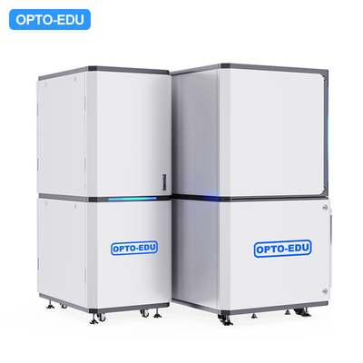
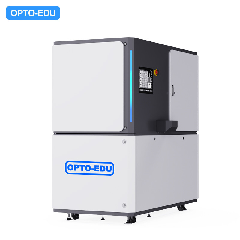
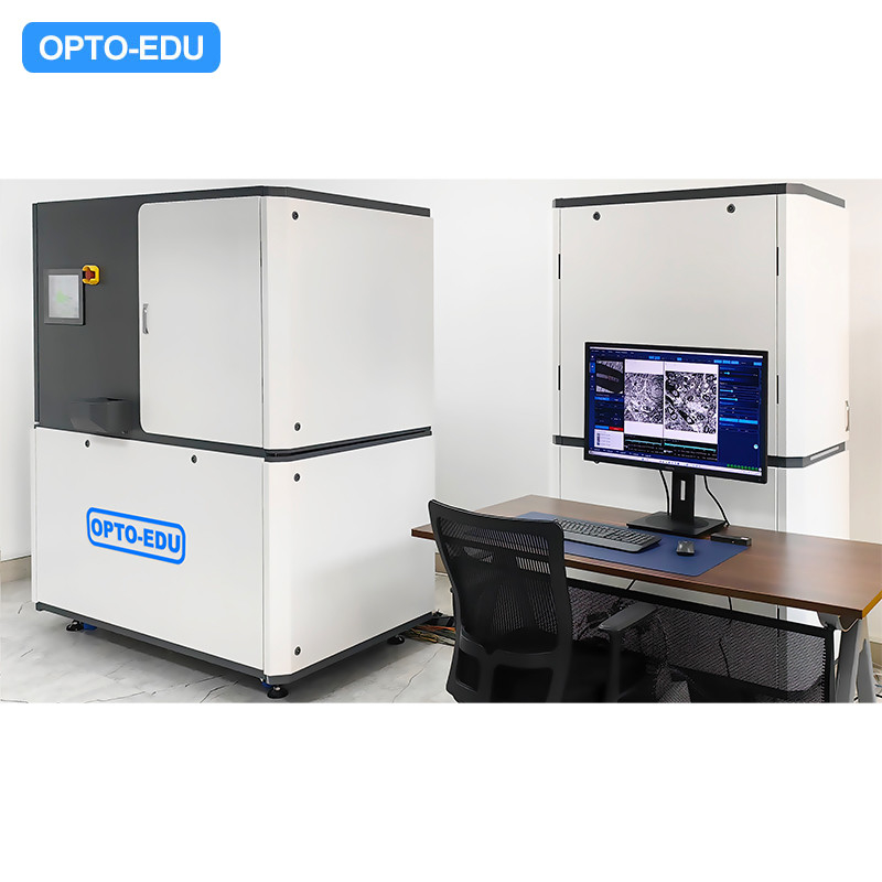
OPTO-EDU A63.7230 Mikroskop Elektron Transmisi Pemindaian STEM 50KV 800000x
-
Modus PencitraanBF/DF (Bidang Terang/Bidang Gelap)
-
Tegangan pendaratan Mode STEM50KV
-
Jenis DetektorDetektor langsung semikonduktor
-
Pistol ElektronEmisi medan termal jenis Schottky
-
Arus balok elektron50Pa hingga 100NA
-
Tahap sampelX = ± 4mm, y = ± 4mm, akurasi posisi 1um
-
Tempat asalCina
-
Nama merekCNOEC, OPTO-EDU
-
SertifikasiCE, Rohs
-
Nomor modelA63.7230
-
Dokumen
-
Kuantitas min Order1 PC
-
HargaFOB $1~1000, Depend on Order Quantity
-
Kemasan rincianKemasan Karton, Untuk Transportasi Ekspor
-
Waktu pengiriman5 ~ 20 Hari
-
Syarat-syarat pembayaranT/T, Serikat Barat, Paypal
-
Menyediakan kemampuan5000 buah/Bulan
OPTO-EDU A63.7230 Mikroskop Elektron Transmisi Pemindaian STEM 50KV 800000x

|
Sistem Analisis Pencitraan Partikel Mikro Otomatis Cepat A63.7230 adalah mikroskop elektron transmisi pemindaian (STEM) yang cepat, cerdas, dan sepenuhnya otomatis dengan hak kekayaan intelektual independen penuh pada 50KV.Ini memenuhi kebutuhan aplikasi di bidang seperti pengamatan morfologi virus, pengujian keamanan bank sel vaksin, penelitian dan manufaktur vaksin, penelitian patologi klinis pada potongan jaringan, dan penelitian biologis pada otak neural connect omics. |
|
A63.7230 Teknologi inti |
|
|
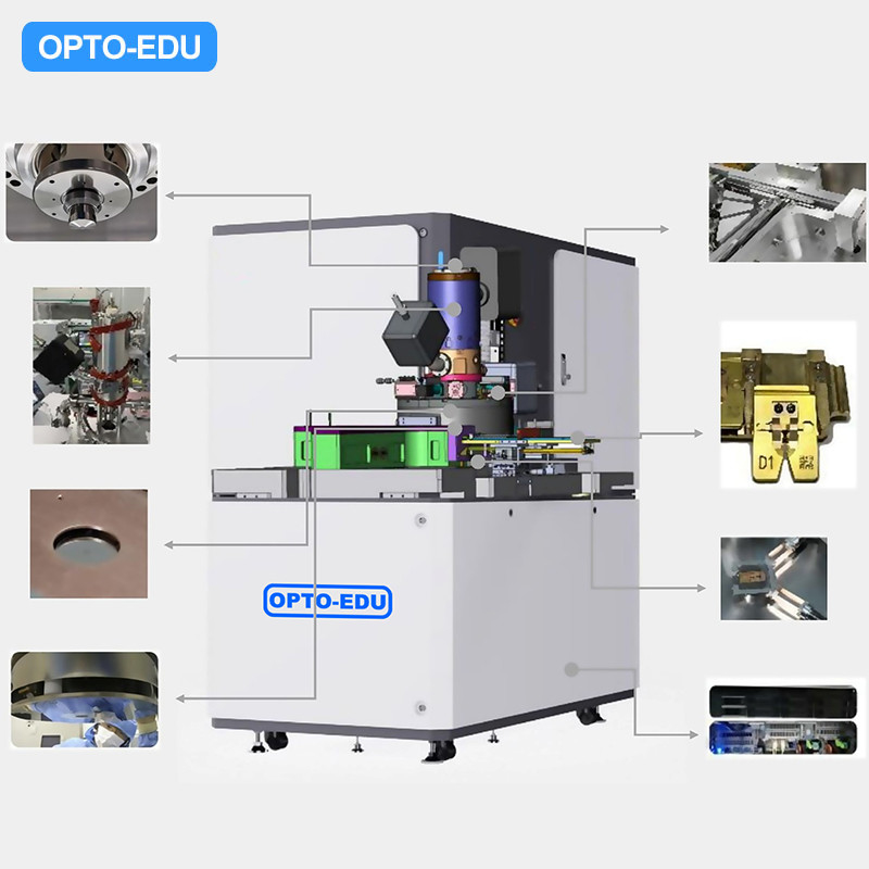
️Sistem optik elektron dengan resolusi tinggi dan kecerahan tinggi 100M/s ultra high speed imaging pada 50KV. Sistem ini memiliki kemampuan analisis tingkat video (25fps@2k*2k) dalam skala nanometer,Memungkinkan pengumpulan informasi sepenuhnya otomatis tanpa penghapusan sambil mempertahankan resolusi tinggi. ️Detektor Elektron Langsung Sensitivitas Tinggi Semua detektor A63.7230 menggunakan detektor elektron langsung yang dirancang secara independen yang mengubah elektron langsung menjadi sinyal listrik,mencapai efisiensi deteksi lebih dari 80% dan rasio sinyal ke kebisingan (SNR) yang lebih tinggi. ️Pergeseran Cepat Antara Bidang Besar dan Pencitraan Resolusi Tinggi Desain optik elektron inovatif memungkinkan pencitraan medan besar dan pencitraan resolusi tinggi untuk beroperasi secara independen, memungkinkan beralih cepat, identifikasi partikel yang tepat dan penentuan posisi,dan gambar resolusi tinggi yang cepat. ️Platform Gerak Mekanis Berkecepatan Tinggi dan Stabilitas Tinggi Menggunakan platform gerak bebas getaran, X = ± 4mm, Y = ± 4mm, akurasi posisi 1um. |
|
| A63.7230 Mikroskop Elektron Pemindaian Transmisi (STEM) | |
| Resolusi | 1.0nm@50kV |
| (1nA arus sinar, dalam kondisi optimal) | |
| Mode Pencitraan | BF/DF (Light Field/Dark Field) |
| Tegangan pendaratan Mode STEM | 50KV |
| Jenis detektor | Detektor langsung semikonduktor |
| Perbesar | 1X-500X (Gambar Optik Peningkatan Rendah) |
| 500X - 800,000X (Gambar STEM) | |
| Senjata Elektron | Emisi medan termal jenis Schottky |
| Arus Sinar Elektron | 50pA sampai 100nA |
| Tahap Sampel | X=±4mm, Y=±4mm, Keakuratan Posisi 1mm |
| Aliran Pencitraan | Dapat menyelesaikan pencitraan area 1x1mm2 pada piksel 4nm dalam waktu 0,5 jam |
| Akuisisi Gambar Ultra-Kecepatan Tinggi | 100MB/s, gambar 24k x 24k hanya membutuhkan waktu 6,5 detik untuk menangkap |
| Metode Akuisisi | STEM Pembelian Medan terang (BF) atau Medan gelap (DF) |
| Perangkat Lunak Kontrol Mikroskop Elektron Berkinerja Tinggi | Dilengkapi dengan optimasi gambar otomatis, pelacakan fokus cerdas, navigasi optik panorama, dan fungsi akuisisi area besar yang sepenuhnya otomatis |
| Pergeseran Cepat Antara Bidang Besar dan Pencitraan Resolusi Tinggi | Desain optik elektron inovatif, operasi independen dari pencitraan medan besar dan pencitraan resolusi tinggi, beralih cepat, identifikasi partikel yang tepat dan penentuan posisi,pencitraan resolusi tinggi yang cepat |
| Perangkat Lunak Pengolahan Analisis Gambar AI Server | Pencitraan medan ultra-besar, 100um@25nm, AI Server pengakuan dan pengukuran efisiensi tinggi |
| Kapasitas Deteksi Kuantitatif Partikel dengan Kinerja Tinggi | Sistem pengisian sampel baru dan sistem manajemen sampel otomatis, memastikan deteksi kuantitatif |
|
▶Sistem optik yang dirancang untuk deteksi partikel mikro otomatis
Mikroskop elektron transmisi tradisional memiliki bidang pandang yang kecil, yang tidak dapat memenuhi kebutuhan deteksi dan identifikasi sejumlah besar nanopartikel.7230 dirancang berdasarkan konsep peralatan deteksi sinar elektron kelas industri semikonduktor, mencapai kemampuan deteksi nanopartikel dengan throughput tinggi.
A63.7230 mencapai pencitraan kecepatan ultra tinggi melalui desain inovatif seperti teknologi pencitraan cepat, tahap sampel bebas getaran, sistem optik elektron kecepatan tinggi, dan teknologi AI,dengan kecepatan pencitraan mencapai lusinan kali dari mikroskop elektron tradisional. |
|
▶Desain Otomatis Serangkaian tindakan seperti inspeksi power-on, posisi navigasi, sentrasi satu klik, penyesuaian fokus, dan koreksi pergeseran otomatis.Sistem pelacakan fokus real-time terdiri dari hardware dan softwareMenggunakan defleksi elektronik yang tepat untuk mencapai posisi gambar sampel yang akurat, menghasilkan pengulangan hasil yang tinggi.Ini tidak hanya menghilangkan kebutuhan untuk upaya yang luas untuk menyesuaikan dan menemukan posisi sampel tetapi juga memanfaatkan kecerdasan buatan untuk deteksi otomatis, akhirnya mencapai operasi terus menerus tanpa pengawasan. |
|
▶Fungsi perangkat lunak yang dapat disesuaikan untuk klien yang berbeda Memanfaatkan kecerdasan buatan modern, algoritma AI, dll, untuk membantu personil eksperimen dalam analisis,dari persiapan sampel front-end untuk pencitraan otomatis bagian penuh dan jahitan dengan mikroskop elektron, menghasilkan peta resolusi tinggi, dan kemudian ke pemrosesan data back-end. analisis cerdas AI dapat digunakan untuk deteksi otomatis dan klasifikasi partikel,menyediakan pengguna dengan solusi lengkap. |
Produk kami dijual di seluruh dunia. Anda dapat yakin dengan seluruh proses produk kami.